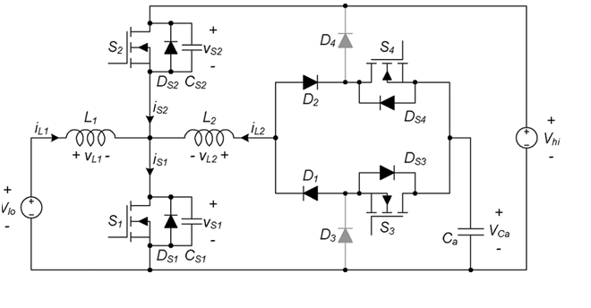
BASIC CIRCUIT

HARDWARE
SIMULATION


zvs in matlab for switch S1
HARDWARE


- BATTERY -4V AND 12V
- Micro controller -dspic30f2010
- drivers -fan7392 and tlp250
- MOSFET -CSD19534 (OR USE IRF540)
- DIODE -BYQ28E
waveforms
zvs waveforms for switch S1


waveforms S1-gate and Vds1 without snubber (no zvs)


waveforms S1-gate and Vds1 with snubber ( zvs)
zvs waveforms for switch S2

waveforms S2-gate and Vds2 without snubber (no zvs)


waveforms S1-gate and Vds1 with snubber ( zvs)

gate waveforms at S1(yellow) and S2(blue)
gate waveforms at S1(yellow) and S3(blue)
gate waveforms at S1(yellow) and S4(blue)
gate waveforms at S2(yellow) and S4(blue)
Design
DUTY CYCLE CALCULATION
Gain = Vhi / Vlo = 14/2 = 7
DUTY CYCLE = 1/(Gain + 1) = 1/(7+1) = 0.125 = 12.5%
DUTY CYCLE (BOOST) = 12.5%
INDUCTOR VALUE CALCULATION
Vout = 14 V
Vlo = 2 V
Vhi = 14 V
Iin = 5 A
Fout = 100 kHz
Fsw = 1000 kHz
Ts = 1 / Fsw = 1 µs
Vout = (Vhi * D + Vlo * (1‑D)) / 2
Vout = 7 V (boost mode)
Gain = Vhi / (2*Vlo) = 14 / 4 = 3.5
D = 1 / (Gain + 1) = 1 / (3.5 + 1) = 0.222 = 22.2%
L = (Vhi – Vlo) * D * Ts / (Iin) = (14‑2) * 0.222 * 1 µs / 5 A = 0.53 µH ≈ 1 µH (standard value)
Auxiliary Inductor design
Is1 = Vhi * ∆Ts / (2 L2)
∆Ts = 1 µs
For boost mode Is1 = 5 A
L2 = 14 * 1 µs / (2 * 5 A) = 1.4 µH ≈ 1.4 µH
Auxiliary Capacitor design
Vca = Vhi / 2 = 7 V
During dead time the current through the capacitor is 5 A
C = I * dt / dV = 5 A * 1 µs / 7 V = 0.71 µF ≈ 1 µF (standard value)
program(mikroc -dsPIC30f2010) (boost operation only)
//crystal of 16 MHz
#define boostgates1   LATE.F0        //S1
#define buckgates2   LATE.F1        //S2
#define snubberlowergates3   LATE.F2 //S3
#define snubberupperergates4   LATE.F3 //S4

void main()
{
    TRISE.F0=0;TRISE.F1=0;TRISE.F2=0;TRISE.F3=0;
    snubberupperergates4=0;
    boostgates1=0;
    snubberlowergates3=0;
    buckgates2 =0;
    while (1)
    {
        buckgates2 =1;snubberupperergates4=1;Delay_us(1);   //s2 & s4 is on   ,time =1
        buckgates2 =0; Delay_us(1);                       //s2 off
        boostgates1=1;Delay_us(11);                       //s2 off, s4 and s1 on,time =12
        snubberupperergates4=0;                           //s4 -off & s1 on   ,time =12
        snubberlowergates3=1;   Delay_us(1);              //s3 on & s1 on   ,time =13
        boostgates1=0;Delay_us(1);                       //s1 off ,s3 on , time =13
        buckgates2 =1;   Delay_us(6);
        snubberlowergates3=0;
    }
}
program(mikroc -dsPIC30f2010) (buck or boost mode using mode switch)
//crystal of 16 MHz
#define boostgates1   LATE.F0        //S1
#define buckgates2   LATE.F1        //S2
#define snubberlowergates3   LATE.F2 //S3
#define snubberupperergates4   LATE.F3 //S4
#define modeswitch   PORTD.F0   //modeswitch

void offallswitches(void);
int time=14,f=0;

void main()
{
    TRISE.F0=0;TRISE.F1=0;TRISE.F2=0;TRISE.F3=0;   //gates as output
    TRISD.F0=1;   //modeswitch
    offallswitches();
    while (1)
    {
        if(f==0)   //boost mode duty
        {
            buckgates2 =1;snubberupperergates4=1;Delay_us(1);   //s2 & s4 is on   ,time =1
            buckgates2 =0; Delay_us(1);                       //s2 off
            boostgates1=1;Delay_us(14); //11                  //s2 off, s4 and s1 on,time =12
            snubberupperergates4=0;                           //s4 -off & s1 on   ,time =12
            snubberlowergates3=1;   Delay_us(1);               //s3 on & s1 on   ,time =13
            boostgates1=0;Delay_us(1);                        //s1 off ,s3 on , time =13
            buckgates2 =1;   Delay_us(4);                     //6
            snubberlowergates3=0;
        }
        else if(f==1)        //buck mode duty
        {
            buckgates2 =1;snubberupperergates4=1;Delay_us(1);   //s2 & s4 is on   ,time =1
            buckgates2 =0; Delay_us(1);                       //s2 off
            boostgates1=1;Delay_us(9); //11                    //s2 off, s4 and s1 on,time =12
            snubberupperergates4=0;                           //s4 -off & s1 on   ,time =12
            snubberlowergates3=1;   Delay_us(1);               //s3 on & s1 on   ,time =13
            boostgates1=0;Delay_us(1);                        //s1 off ,s3 on , time =13
            buckgates2 =1;   Delay_us(4);                     //6
            snubberlowergates3=0;
        }
        if(modeswitch==0)
        {
            offallswitches();
            if(f==0) f=1; else f=0;
            Delay_ms(1000);
        }
    }
}

void offallswitches(void)
{
    snubberupperergates4=0;
    boostgates1=0;
    snubberlowergates3=0;
    buckgates2 =0;
}